Research themes
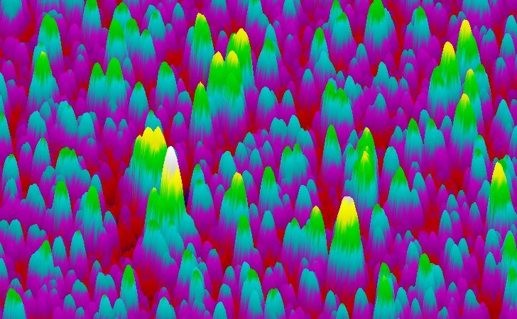
Nanostructures
Nanoparticles and nanotechnology
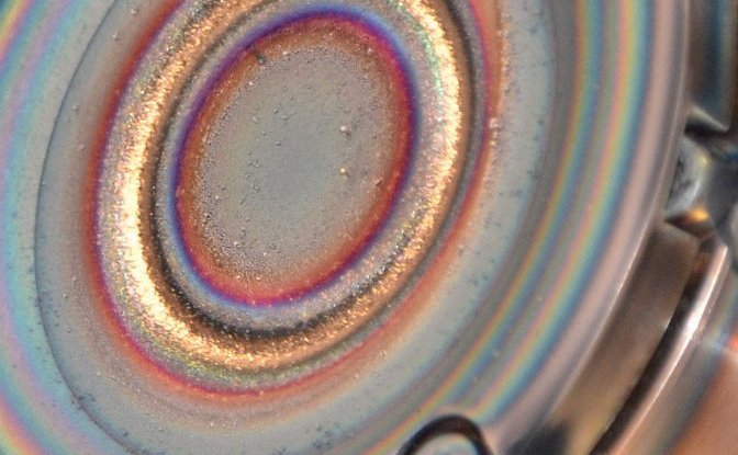
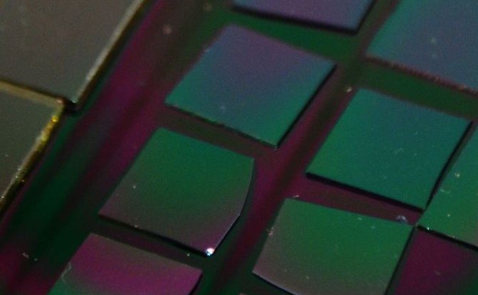
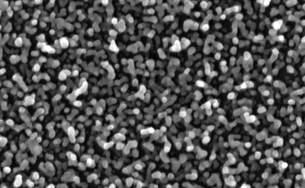
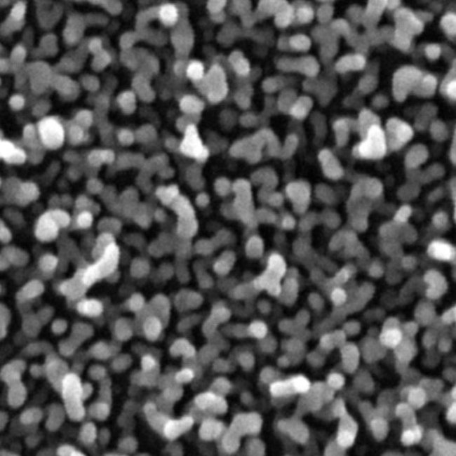
Nanostructured surfaces consist of objects with lateral size 10 ‑ 100 nm. Nanostructured interfaces have gained enormous importance in view of the possibility to utilize deliberately modified physical, chemical or bio-responsive features without affecting the bulk material. We used to study and deposit surfaces of isolated nanopraticles, nanoislands formed by coalescent coagulation, and homogeneous surfaces with nanotexture. In our case the nanoparticles are prepared by gas-phase aggregation synthesis which enables precise size selection and defined manipulation resulting in homogeneous surface distribution. Beside investigation of elemental processes and nanostructure growth we namely prepare the films for (bio) sensors utilizing phenomena of LSPR (localized surface plasmon resonance) or SERS (surface enhanced Raman spectroscopy). Our current challenges are core-shell nanoparticles, nanocomposites and nanoparticle manipulation.
TOPICS / HIGHLIGHTmore_vert
Currently running research topics
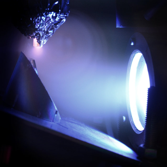
pre-ionized HiPIMS discharges
discharges with high fraction of ionized species running at very low pressure
Highlight publications
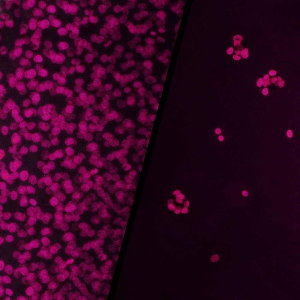
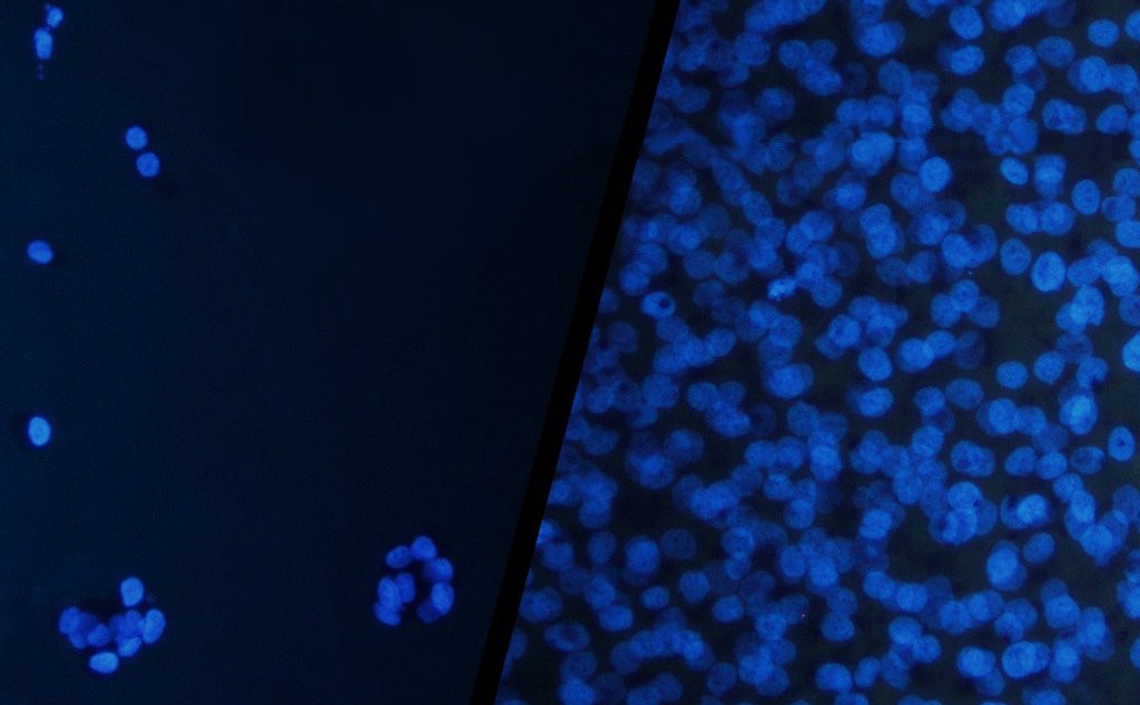
Bio-surfaces
Bio-functional surfaces and films for (bio)sensors
We develop and study surfaces with vision to be used in a direct contact with living tissue. For example, modification of implant surfaces for enhance attachment of selected molecules, proteins or cells are studied. Beside of it we investigate and deposit the surfaces enriched by chemical grafts (to prepare chemically active interfaces for e.g. sensors) or surfaces doped by defined molecules (e.g. antibiotics). Bio‑functional thin films are prepared by plasma sputtering of both metallic as well as polymer materials. Than amine (‑NHx), carboxyl (‑COOH), carbonyl (‑C=O), fluorine‑containing (‑CFx), hydroxyl (‑OH) etc. groups rich surfaces are prepared directly during the deposition. We closely collaborate with Laboratory of Glycobiochemistry to study the response of bio‑molecules onto a tailored thin film.
TOPICS / HIGHLIGHTmore_vert
Currently running research topics
plasma diagnostics of pre-ionized discharges
in-situ time-resolved diagnostics during deposition of thin films
Highlight publications
Industry
High-tech coatings with high added value
Our laboratory closely collaborates with industrial partners in frame of joint projects. Our typical role is to develop and optimize functional thin films, including the suitable methodology. Hard protective coatings, films to chemically aggressive environment, anti‑fouling, hydrophobic, temperature resistant, photocatalytic, anticorrosive films etc. are the examples. Plasma vapour deposition (PVD) and plasma enhanced chemical vapour deposition (PECVD) are most often used methods with respect of high efficiency required by the technological process. Furthermore, application and optimisation of discharges together with surface plasma treatment is also included in our portfolio.
TOPICS / HIGHLIGHTmore_vert
Currently running research topics
antimicrobial surfaces with immobilized bio‑functional molecules
advanced research of oxide films - TiO2, SiO2
optically-transparent and electrically conductive films for biosensors
Highlight publications
Plasma
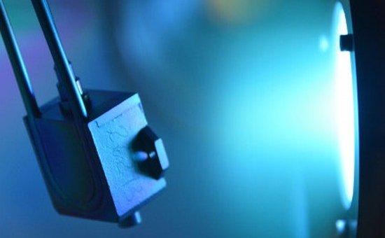
Low-temperature plasma sources development and diagnostics
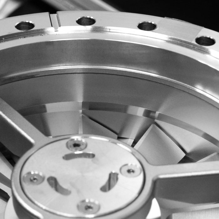
We develop, optimize and modify the plasma sources for physical vapour deposition (PVD) and plasma enhanced chemical vapour deposition (PECVD) processes. PVD processes typically employ planar magnetrons and hollow cathode sputtering running in dc, dc‑pulse‑modulated and rf modes. High power discharges are used for production of dense plasma with large fraction of ionized sputtered material. Optimised input parameters of the discharge allows tailoring of film properties and surface morphology. We pay attention to film crystallography, surface morphology, optical and electrochemical properties that can be tailored by precise monitoring of internal discharge parameters (power and species flux, chemical composition of working atmosphere, plasma density etc.).
TOPICS / HIGHLIGHTmore_vert
Currently running research topics
deposition of metal, metal‑oxide and nanostructured composite films
investigation of the cluster growth